Electron Beam Lithograph System
Electron Beam Lithograph system is one of the technologies to form the fine patterns by using electron beams in order to make the integrated circuits for semiconductor etc. This Lithograph System possesses especially the several features such as the ultra thin-line lithography, the laser-assisted position-detector with high precision and high stabilization, and the high-speed and wide-area patterning. For instance, high focusing of electron beams enables to form the fine pattern with a minimum line width of 10 nm. In addition, the system attains the high precisions in the beam-position-decision of minimum 0. 31 nm by use of 18 bit DAC (Digital to Analog Converter), and in the stage-position-reading of 0. 6 nm by using the Laser Interferometry.
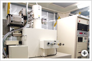

The process of the lithography is first to coat the photo-resist on the sample surface with uniform thickness by spin-coater, and then to lithograph the pattern by using electron beams and to develop it, and thus to form the targeted resist pattern. The thickness of resist is controlled by the revolution of spin-coater. The System was installed in the clean booth unit under class-100 in order to realize an accuracy of lithography with nano-meter scale. The circumstance of the System is considered so as to minimize the influence of the surroundings such as vibration, noise and magnetic field by means of various ways, such as inducing the seismic isolation floor structure at the time of the design of HTRC, the active removal-vibration-stand appended in the system, and magnetic shield by permalloy metal. The booth has lighting system covered by UV absorption film due to the use of resist which is sensitive to the UV lighting and is also furnished with the window glass covered by UV-cut film.
Model
ELS-7500EX (ELIONIX CO. , LTD)